
'Like uprooting tree stumps' – a simpler method to manufacture biosensors
27.8.2026 15:42:00 CEST | KTH Royal Institute of Technology | Press Release
A new manufacturing method could help move the production of nanoscale sensors from specialized fabrication facilities to conventional semiconductor manufacturing plants.
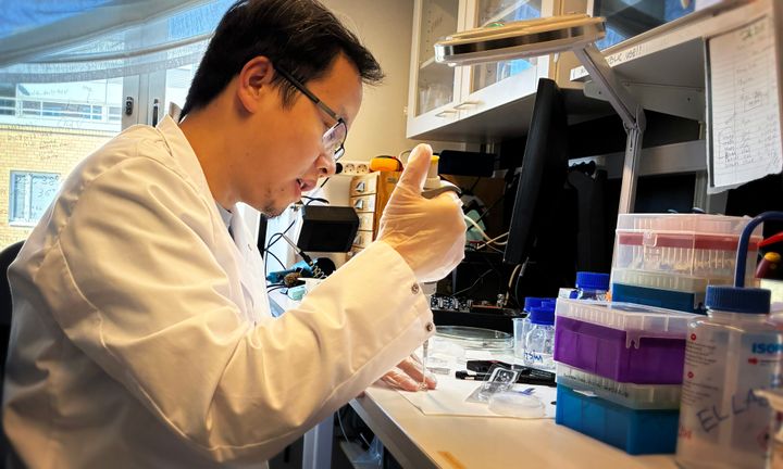
Publishing in Science Advances, researchers from KTH Royal Institute of Technology liken their technique to uprooting a tree stump with rope.
The work aims at solving a bottleneck in fabricating nano-scale holes in thin membranes, a key component in a range of sensing and analysis technologies used in medical research and, increasingly, in specialized clinics where sequencing systems are used for outbreak surveillance, cancer genomics or infectious disease identification, among other things. Nanopores are valuable tools in these settings because their extremely small openings in ultra-thin materials can be used to detect and analyze individual molecules such as DNA and proteins.
Frank Niklaus, professor of micro and nanosystems at KTH Royal Institute of Technology, says the study demonstrates the unique approach of using built-in mechanical stress to create nanoholes.
A typical sensor device membrane has a single nanopore, which acts as a single molecule detector. These openings are produced one-at-a-time, using slow, expensive or difficult-to-scale nanofabrication techniques, such as electron-beam drilling and Transmission Electron Microscope (TEM) sculpting, says Xinxin Liu, a doctoral student at KTH Royal Institute of Technology and first author of the study.
But the study demonstrated that this technique can produce large arrays of nanopores in parallel by harnessing fracture mechanics generating openings as small as about
6-10 nm.
The process begins with a stack of layers placed on a silicon wafer. The top layer is deliberately stretched under tension. Underneath is a second layer of material that will be etched away until a small pre-defined shape remains, which is meant to define the shape of the nanopore in the third layer of material underneath. This third layer is the sensor membrane in which the nanopore will be formed.
“The beam pulls on until it tears a nanoscale fragment from the membrane, creating the hole,” Liu says. “Much like a removing a tree stump with a rope – the beam attaches to the nanoscale anchor, pulling it away from the membrane, which serves as the ground.”
The technique was tested successfully in multiple materials, including dielectric, metallic and semiconductor sensor membranes. The study showed these nanopores were effective at DNA analysis and molecule detection.
Liu says the researchers have patented the technique and formed a startup to progress it toward commercial implementation. “We have already shipped samples to a collaborator for testing, so it has moved beyond the lab stage.”
Contacts
Xinxin LiuKTH Royal Institute of Technology
xinxinl@kth.seImages
Links
Subscribe to releases from KTH Royal Institute of Technology
Subscribe to all the latest releases from KTH Royal Institute of Technology by registering your e-mail address below. You can unsubscribe at any time.
Latest releases from KTH Royal Institute of Technology
Now multiple optical devices' stabilizing properties can be identified with a single reprogrammable chip14.10.2026 13:03:08 CEST | Press Release
In optical fibers, chips and other light-guiding devices, minor defects can scatter photons and disrupt their path. A new study demonstrates a way to reveal properties which, in certain systems, help light wave behavior withstand such flaws. The method could help speed up the search for new kinds of electronics and optical technologies, and contribute to more reliable quantum devices.
Researchers identify aggressive molecular features in low-risk prostate cancer7.10.2026 13:41:39 CEST | Press Release
A new study revealed molecular features linked to more aggressive prostate cancer in a subset of patients who had been classified as low risk, highlighting biological differences that may not be apparent from clinical measures alone. The results could lead to new therapeutic strategies.
Why do spruce take decades to reproduce? A genetic study offers new clues14.9.2026 17:41:41 CEST | Press Release
New techniques have enabled researchers in Sweden to begin decoding how one of Northern Europe's most important coniferous tree species switches from growing branches to producing cones – their seed-bearing reproductive organs.
KTH builds Swedish expertise in nitrocellulose2.9.2026 12:54:32 CEST | Press Release
Sweden wants to reduce its dependence on foreign suppliers for nitrocellulose, a raw material central to the production of conventional propellants. KTH is now launching a new competence centre to build up expertise across the entire chain – from forest-based raw materials and manufacturing to safe storage.
Technique could make flat optic fiber 1,000 times more sensitive than standard fiber13.8.2026 10:57:20 CEST | Press Release
Optical fiber has already transformed the modern world. New research now suggests it could do even more. A new flat fiber fabrication technique produces a high fidelity sensor for a wide range of applications, from batteries to bridges, according to a recently-published study.
In our pressroom you can read all our latest releases, find our press contacts, images, documents and other relevant information about us.
Visit our pressroom